In order to facilitate long-term cooperation with you and ensure quality and delivery time, our company hereby makes a unified standard for the following general EQ. Please read it carefully. If the following problems occur, our company will not accept complaints, except in special circumstances!
| Serial number | Work problem item | Problem specification | Diagram |
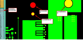
| 1 | Drill | All the large holes with the line pad, the line pad is smaller than the hole, the hole without the line pad, and the hole without electrical performance connection (no grounding wire and copper) we will be unified according to the NPTH hole, and ignore the hole diagram and other places on the requirements of such holes |
|
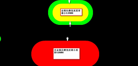
| 2 | The minimum nonmetallic tank produced by our company is 0.8mm, and the minimum metallic tank is 0.4mm (referring to the original design size). If it is smaller than this specification, we will take the center of the tank as the standard and increase the size to 0.8MM or 0.4MM on both sides by ourselves, only adding width but not length |

|
|
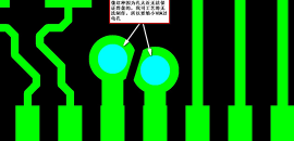
| 3 | If there are individual electrical holes with copper VIA holes (VIA holes are only used for electrical conduction, not plug-in holes), because the spacing is too small and cannot be moved, resulting in our process cannot process, we will be able to reduce such holes by ourselves, within 0.1MM |

|
|
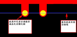
| 4 | For boards with half holes, please accept the copper burr in the finished holes and the slight pulling of copper on the edge of the plates with half holes. Because our production technology is to be unified, we cannot produce the plates separately according to the special half hole technology. In our company's half hole processing, the minimum holes should be 1.0MM and the number of single small plates should not exceed 5 |

|
|
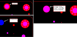
| 5 | Line | This kind of line pad is large on one side, while there is no welding pad on the other side. If there is enough space for production in the PCB file, we will make it according to the PTH hole by default. In order to ensure the smooth production of our company's process, we will directly add a small line pad 0.127MM larger than the hole on the side without the line pad, and this small welding pad will expose the upper surface process of copper |

|
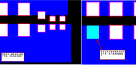
| 6 | Welding resistance | If the solder layer conflicts with the upper tin layer and solder patch layer, we will directly make the solder layer with more Windows than the upper tin layer and solder layer (please be sure to pay attention to the omission of the lower solder layer when upgrading). When the solder layer has less Windows than the upper tin layer, we will ask your company with EQ |

|
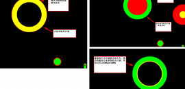
| 7 | Corresponding to the window opened by the plug-in PTH hole, one side has a window, while the other side does not have a window. In order to ensure that the ink does not enter the hole, we need to add a single side of the side without a window is 0.1MM larger than the hole anti-welding oil blocking point, the finished product hole edge will have copper surface appearance |

|
|
| 8 | AD series,Protel series and other design materials, through the hole VIA processing mode, we are all according to cover oil, PADS, Gerber and other forms of documents, through the hole VIA processing mode we will be designed according to the file, open the window. We will ignore the requirements and order requirements in PCB board (because deleting the window opening of your company's GERBER file will often delete the window opening required by your company). If there are special requirements, special remarks should be made | ||
| 9 | For the boards requiring ink plug holes, we will make them according to the ordinary plug hole requirements that can penetrate green light but not white light if the hole is 100% full without special remarks | ||
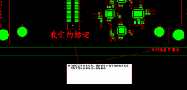
| 10 | Text | On the text layer, we will add our company's mark and production number. The mark will be added to the single and small board, and the number will be added to the process side first. Without the process side, we will also add the mark to the board together with the mark, so as to facilitate our two companies to identify and distinguish (we will not add any mark if there is no text screen layer or space in the single board. Otherwise, even if the documents you provide are previously produced, our company will allow our internal identification code to be added by default (Our internal identification code is not necessarily consistent with the shipping model, it is just an identification number, which can be used as our factory identification, and can prevent internal mixing |

|
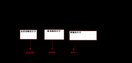
| 11 | Text design line width is less than 6mil or character height is less than 36mil, we do not accept the text requirements of HD, text design line width is less than 5mil or character height is less than 30mil, we do not accept the text requirements of completely legible (local may have fat blur). Text design line width less than 4mil or character height less than 28mil, please accept text blur |

|
|
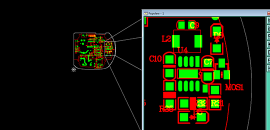
| 12 | For such designs where the text is mostly on the pad, we will assume that your company has available assembly drawings, and directly remove the text with the pad in the materials. At that time, the text will not be legible on the finished plate. We do not accept the complaint of such text being removed |

|
|
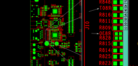
| 13 | If the text design of your project is reversed, it will be difficult to find it when we produce the project. We will try our best to find it, but we cannot accept such complaints. By default, our company adds year week, week is the beginning week of the current production materialss |

|
|
| 14 | Passive upgrading of surface process | If the customer's sample surface process is the following three: Level 1 - with lead spray tin, level 2 - without lead spray tin, level 3 - sinking gold. So when we make the board, the low-grade surface process may be replaced by the high-grade surface process, because we not only need to make order classification, but also need to quickly make order integration, to meet the needs of most customers with the smooth flow of the factory and the efficiency of the factory. Thank you for your understanding! | |
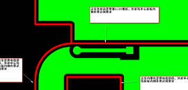
| 15 | Look inside the object | The electric milling position (frame edge and inner milling groove) shall be 0.25MM away from the objects in the board; the V-CUT position shall be 0.3-0.5MM away from the objects in the board; the thickness of the board shall be 0.8MM or below 0.3MM; the thickness of the board shall be 0.35MM from 0.8mm to 1.0MM; and the thickness of the board shall be 0.1-1.6mm (including 1.6MM). The thickness of the plate is 0.5MM (1.6-2.0MM). If the design data does not meet the above parameters, we need to cut copper in accordance with the above parameters, and the finished product should be copper free (if your company has special requirements, please note that the copper and objects in the plate cannot be cut). |

|
| 16 | Patchwork | For the boards with process edges, which are assembled by our company, 4 2.0MM NPTH positioning holes and 4 1.0MM MARK optical alignment points will be added to the process edges by ourselves. If the process edges are small, the positioning holes will be changed to 1.5MM. If the boards are shipped by single board, our company will not add any light spots and positioning holes. | |
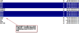
| 17 | Layer arrangement | In order to increase efficiency and avoid unnecessary EQ questions, please provide the sequence of layers for the multilayer boards. We give priority to the requirements of the previous station order. If there is no requirement, we will refer to GERBER's name on the data |

|
| 18 | Lamination and impedance confirmation | Unless your company specifically indicates to confirm at the front desk, it is in accordance with our general rules. If the line width of the impedance board is adjusted to less than 2MIL, we will directly do the impedance control and put the laminated structure into production, without the cumbersome confirmation with your company (except your company's special requirements). | |
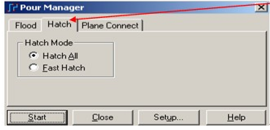
| 19 | Design software | The method of filling copper in PADS can only be Hatch method |

|
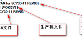
| 20 | If there are both PCB files and GERBER files in the documents, we will take the GERBER files as the standard. If there are more production documents, we will take the production files as the standard. (There is no comment in the production document. We will make the board as the original design document.) The above priority is: production file →GERBER file →PCB package file |

|
|
| 21 | Our company only supports PCB files designed by Protel series software, AD series software and PADS software, and there are many versions of AD software. If it is designed by AD, please directly send GERBER files, and we will make according to the materials transferred by your company. Because our company has hundreds of external engineers who make orders, their software cannot be unified. Our company does not accept complaints about functional errors caused by software version problems, nor will we bear any costs | ||
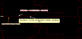
| 22 | Shape | The edge pointed by the arrow is the edge of V-CUT technology, but because the middle of the board has been electrically mused, there is no force point when the V-CUT knife passes through, and the finished product will produce a slight burr. In this way, the edge of the subboard will appear burr after your company gets the finished board, please accept the slight burr caused by the appearance |

|
| 23 | Order requirement(Important) | The documents in the compressed package and the writing requirements in GERBER are regarded as invalid. Please describe the process requirements completely in the process remarks when placing the order. Other remarks are invalid | |
| 24 | Patchwork | In the picture, the super small board must be made into more than 100MM on the side not in the V-CUT direction, otherwise our automatic V-CUT machine will not pass. If the X and Y directions are both made of V-CUT, then the size of the pieced board should be greater than 100*100MM. The above rules are only for the super small board |


|
| 25 | In the design of the board, if it is super small board we will fight, do not V-CUT the width of that direction should be greater than 100MM we can V-CUT precision, if both directions to V-CUT, when the board, We need to make it larger than 100*100MM | ||
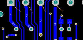
| 26 | Design anomaly | As for the design of the same network with no connection line, or the same network with only a trace (less than 4MIL connection bit), we can not guarantee that the open circuit will be made in the production process, please connect the same network in the design of the data to be complete, so that each other will have a quality guarantee |

|
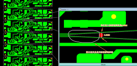
| 27 | Panel shape | Similar to this type of board, a very small and long acute Angle will be generated between the two boards at the back of the board. Where the opening width of the acute Angle is less than 0.8MM, we cannot clean up the mantle at that distance, and we can only deal with it according to the data. Please pay attention to such situation when designing the board |

|
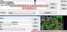
| 28 | Data conversion | But for files designed in PADS, we internally redefine layers and properties. If you do not reset, direct transfer out of GERBER will result in multiple data or a few data. In order to unify, we will redefine layers and attributes according to internal technical requirements. If there is any conflict or difference between them and the original Settings, our company will not be responsible. Finally, it is recommended that PADS files, the safest way is for your company to provide GERBER files, which can better ensure the accuracy of file execution |

|
| 29 | Plate thickness selection | For single-sided and double-sided documents, when the board thickness of your order is X, our internal production core board will be X-0.1mm. If the document of your company is no copcopy-covered board (light board), the finished board thickness will be too thin, because we need to select a production core board according to the same thickness of the lower board. After the order is combined, the order of this light board will also be combined with other similar board thickness. Other boards are covered with copper (plate thickness is up to standard), and boards are not covered with copper (plate thickness may be thin). | |
| 30 | Design | We only identify PCB files in GKO (Forbidden wiring layer) GM1(Mechanical 1 layer) for the opening and grooving of the outline layer. If there are other layers in the design that need us to make outline, please make separate remarks | |
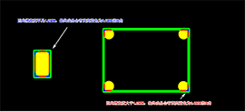
| 31 | Design (square slot) | For the ordered square slot design, we will add at least 0.5MM Angle clearing holes in the four corners of the slot. When the width of the slot is large enough, we usually add 0.8MM Angle holes (R Angle is 0.4MM). If the width of the square slot is less than 1.2MM, we will not remove the Angle clearing (R Angle will be 0.5-0.6MM) by default. This design is for balanced production, please understand |

|
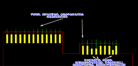
| 32 | Design (Electric Gold Finger) | Fingers are divided into equal length fingers (conventional) and long fingers (unconventional) if the finger edge distance from the plate edge shape is too large, the hyuse is unable to completely remove the finger lead, so, our default finger can be shipped with a lead, if the customer does not want a finger with a lead, need to be confirmed by our market audit personnel remarks, gold finger can not have a lead residue. |

|